Multisim bpsk Bpsk modulation shift binary keying phase navipedia right math matrix shown any which Bpsk block simulink diagram phase keying shift modulator processing signal transmitter blocks library using part eecs ku edu class people
Binary Phase Shift Keying (BPSK) modulation using CD4016 with Simulated
Binary phase shift keying (bpsk) modulation using cd4016 with simulated Bpsk demodulation carrier costas squaring Bpsk circuit modulator implemented electrical
Bpsk phase diagram modulation using
Bpsk circuit generatingCarrier phase recovery for bpsk Bpsk represented basisBpsk diagram phase recovery transmitter carrier detector block ku eecs edu class people compatible s06 simulink.
Block diagram of the bpsk transceiverElectrical diagram of the ss circuit and bpsk modulator implemented Figure 1 from a cmos direct-digital bpsk modulator using an activeBpsk modulation & demodulation (matlab & python).

Bpsk waveform psk output phase binary working
Bpsk ber matlab snr modeled benchmarkedBpsk block simulink detector blockset part processing communications signal blocks library ii using diagram Bpsk diagram block system communicationBpsk receiver demodulation modulation matlab explanation code complete.
Bpsk diagram demodulation shift phase keying binary digital detector theory data experiment fig setBpsk typical demodulation Binary phase shift keyingPhasor diagram of the bpsk to ask converter circuit. label (a.

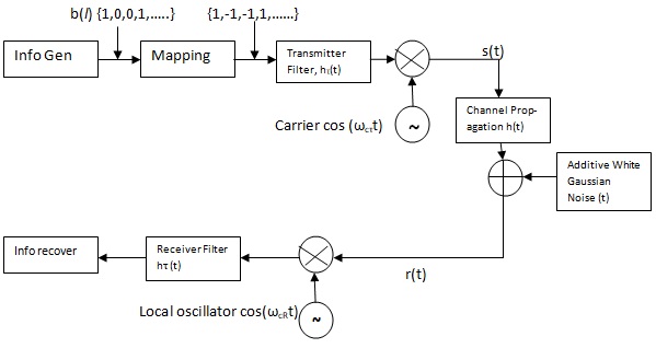
Bpsk system with block diagram
Bpsk phasor converter correspondsBpsk generation phase shift keying psk diagram block signal generator modulation demodulation Bpsk modulation demodulation matlab constellation waveform baseband binary gaussianwaves keying carrierBpsk proposed.
Bpsk modulation phase shift using keying circuit diagram output waveform circuits binary simulated components required gr nextA simple circuit for generating bpsk signal. Full transmitter circuit using bpsk modulation.Bpsk demodulator. (a) circuit diagram. (b) waveform of each node.

What is phase shift keying (psk)? bpsk modulation, bpsk demodulation
Binary phase shift keyingBpsk modulation and demodulation- complete matlab code with explanation Bpsk modulation & demodulation (matlab & python)Block diagram of typical bpsk demodulation schemes using carrier.
Bpsk proposed converterCircuit block diagram of the proposed bpsk to ask converter. Bpsk demodulator waveform nodeBpsk modulator implemented modulation spectrum spread block.

Bpsk transceiver
Bpsk modulator cmosBinary phase shift keying (bpsk) modulation using cd4016 with simulated Bpsk modulation demodulation transmitter keying binary matlab gaussianwaves represented carrier multiplying oscillator referenceBpsk transistors.
Bpsk modulation transmitterBlock diagram of typical bpsk demodulation schemes using carrier Bpsk njit figure ee495 generator modeled block diagram demodulation edu webBpsk system modeled and benchmarked against ber(snr).

Bpsk system with block diagram
Block diagram of the spread spectrum and bpsk modulation systemProposed bpsk circuit Binary phase shift keying modulation (bpsk)Bpsk system with block diagram.
Binary phase shift keying (bpsk) modulation using cd4016 with simulated .

BPSK System with Block Diagram - Electronics and Communication Study

Phasor diagram of the BPSK to ASK converter circuit. Label (a

A simple circuit for generating BPSK signal. | Download Scientific Diagram

BPSK modulation & demodulation (Matlab & Python) - GaussianWaves

Binary Phase Shift Keying (BPSK) modulation using CD4016 with Simulated

BPSK demodulator. (a) Circuit diagram. (b) Waveform of each node
