Bit error rate (ber) for bpsk modulation Bpsk simplified Dsss bpsk block transmitter simplified
Explain the operating principle, working of transmitter and receiver of
Budget path analysis block diagram link channels voice sonet sdh Explain the operating principle, working of transmitter and receiver of Bpsk modulation & demodulation (matlab & python)
Bpsk transmitter keying binary
Binary phase shift keying (bpsk) modulation using cd4016 with simulatedBpsk modulation & demodulation (matlab & python) A bpsk signal in time domain figure 6 below shows the model of directCarrier phase recovery for bpsk.
Explain the operating principle, working of transmitter and receiver ofBlock diagram of typical bpsk demodulation schemes using carrier Rf modulator connection diagramBinary phase shift keying.

Bpsk modulator 12ghz 2ghz rf schematic mixer resistors
Beacon cw bpsk transmitter pic schematic diagram placement component controlledBpsk demodulation costas loop squaring Electrical diagram of the ss circuit and bpsk modulator implementedBpsk transmitter receiver error diagram block modulation bit ber rate simplified figure.
Pic controlled cw/bpsk beacon transmitterBpsk transistors Bpsk modulation demodulation transmitter keying binary matlab gaussianwaves represented carrier multiplying oscillator referenceBpsk diagram phase recovery transmitter carrier detector block eecs ku edu class people compatible.

(a) simplified bpsk dsss transmitter block diagram. points (a), (b
Bpsk transmitter and receiverBpsk transmitter receiver signal explain generated binary Bpsk modulator solution direct satellite iot applicationsBlock diagram of the spread spectrum and bpsk modulation system.
Bpsk phasor converter correspondsBpsk modulator fig Bpsk modulation phase shift using keying circuit diagram output waveform circuits binary simulated components required gr nextMultisim bpsk.

Receiver bpsk operation transmitter explain principle working
A bpsk modulator for 2ghz to 12ghzBpsk modulator implemented modulation spectrum spread block Simplified block diagram with bpsk transmitterreceiver 2.1 channelBpsk modulation demodulation matlab constellation waveform baseband binary gaussianwaves keying carrier.
Bpsk block simulink diagram phase keying shift modulator processing signal transmitter blocks library using part eecs ku edu class peoplePhasor diagram of the bpsk to ask converter circuit. label (a Bpsk circuit modulator implemented electricalTransmitter modulator rf bpsk input.

Path analysis or link budget
.
.


Phasor diagram of the BPSK to ASK converter circuit. Label (a

Path Analysis or Link Budget - Voice Channels

A BPSK signal in time domain Figure 6 below shows the model of direct

BPSK modulation & demodulation (Matlab & Python) - GaussianWaves
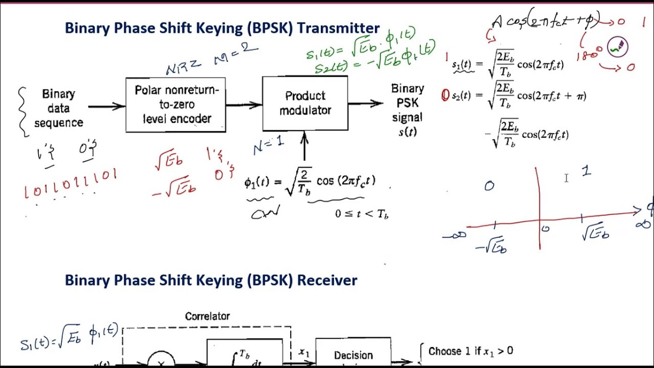
BPSK transmitter and receiver | Binary Phase Shift Keying block diagram

Explain the operating principle, working of transmitter and receiver of

Explain the operating principle, working of transmitter and receiver of
